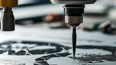
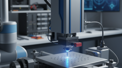
The 2026 market for laser SiC is not defined by one machine or one beam source. Buyers must match the process to the material, component geometry, and production volume. Yole Intelligence’s Power SiC 2023 report projected the SiC power-device market would grow from about $2.7 billion in 2022 to $9.2 billion by 2028. That growth raises practical questions: Can a system cut wafers cleanly, remove material at scale, or create precise grooves without unacceptable edge damage?
The answer depends on the laser type and the task. Nanosecond systems may suit cost-sensitive workflows; ultrafast lasers can limit heat effects in demanding precision work. These are starting points, not guarantees. Test results matter. A polished sample can hide subsurface cracks, while a neat kerf may still reduce usable yield. As SiC materials researcher Dr. Sima Dimitrijev’s published work emphasizes, device performance depends on the material’s properties and how they are managed. For laser processing, that means buyers should evaluate wavelength, pulse duration, throughput, and post-process inspection together.
This guide compares the top laser SiC types for global buyers in 2026, from wafer slicing and dicing to surface texturing. It also flags trade-offs often missed in sales specifications: consumable costs, cooling needs, maintenance access, and integration with existing lines. One caution remains. Published market forecasts describe demand, not guaranteed returns for any individual factory. The strongest shortlist begins with measured samples, transparent process data, and a clear definition of acceptable damage.
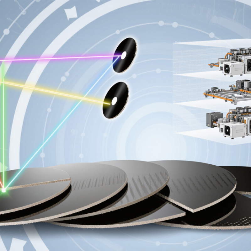
Silicon carbide, or SiC, is a hard ceramic semiconductor used in power electronics, seals, and high-temperature components. In laser materials and processing, “laser SiC” does not describe one universal grade. Buyers may encounter single-crystal wafers, polycrystalline parts, or sintered ceramic, each with different grain structure and performance. The right choice depends on the component and the process.
Lasers can mark, texture, cut, or drill SiC without a conventional cutting tool. A short-pulse beam can remove material in small increments, which helps create fine features on a wafer or ceramic plate. But SiC’s hardness is only part of the challenge. Its thermal conductivity and brittleness affect how heat spreads and how cracks may form. Settings that work on one grade may not transfer cleanly to another. That matters.
For procurement, ask for the SiC form, purity, dimensions, and surface finish, then confirm how the part will be processed. A polished single-crystal wafer behaves differently from a porous sintered component. Test coupons can reveal edge chipping, roughness, and heat-affected zones before full production. Results still vary with wavelength, pulse duration, focus, and fixturing. Laser processing can be precise, but it is not automatically damage-free. Even a neat-looking cut may need inspection under magnification.

Representative room-temperature bandgap values for common silicon carbide polytypes. Bandgap affects a material’s optical and electronic behavior, but laser absorption and processing also depend on wavelength, surface condition, defects, and processing parameters.
Values are representative; reported values can vary slightly with measurement conditions and material quality.
2026 Top Laser SiC Types for Global Buyers
How Laser-Related SiC Types Are Classified
Laser-related silicon carbide is not one universal material grade. Buyers usually compare it by crystal polytype, electrical behavior, orientation, and surface finish. The common polytypes include 4H-SiC and 6H-SiC, with different crystal structures and properties. Conductivity also matters: semi-insulating material and conductive material serve different device and process needs. A polished wafer may suit optical inspection, while a rougher surface can behave differently during laser marking or machining. Ask suppliers for measurable specifications, not just a type name.
Tips: Match the classification to the laser task. Check wavelength, pulse duration, and intended feature size against the material data. Confirm wafer orientation, thickness, doping or resistivity, and surface roughness in writing. Small variations can affect heat flow and the consistency of a cut or mark. Test a sample under your actual settings before ordering at scale.
These categories help narrow choices, but they do not predict every result. Laser response also depends on beam focus, power density, and cooling conditions. A label such as “4H” cannot tell you how cleanly a specific lot will process. That distinction is useful, though not perfect. Record the settings and inspect edges for chipping, discoloration, or cracks. When results differ between batches, revisit both the material certificate and process setup.
Crystal structure & defects For laser applications, SiC grade selection starts with crystal structure and defect control. 4H-SiC and 6H-SiC are hexagonal polytypes; 3C-SiC is cubic. Their optical response and electrical behavior differ, so a grade suitable for a power device may not suit a laser window or precision-machining target. Harris’s widely cited review, Properties of Silicon Carbide, documents these polytype-dependent characteristics. Check the actual wafer specification, not just the “SiC” label.
Thermal performance Thermal conductivity matters when a focused beam deposits heat in a small spot. Published material-property compilations place high-quality hexagonal SiC near 400–500 W/m·K at room temperature, though defects, doping, and measurement direction can shift results. That helps spread heat. It does not guarantee a clean cut. Surface roughness, micropipes, inclusions, and polishing damage can still trigger uneven ablation or edge chipping. Small flaws count.
Verification & testing For transparent or semi-insulating grades, verify wavelength-specific transmission, resistivity, and surface finish in the supplier’s test report. A room-temperature value alone is not enough; laser pulses can create local thermal gradients. SEMI’s substrate standards help buyers compare dimensional and inspection criteria, but they do not replace application testing. Request a sample, measure its absorption at the working wavelength, and inspect the kerf under magnification. Even good data leaves some uncertainty.
Laser processing of silicon carbide varies by wafer stage and factory need. Stealth dicing focuses a laser inside the wafer, creating a fracture path for later separation. It suits thin power-device wafers, where reducing edge chipping matters. Surface scribing and ablation remove material or define patterns; these methods support wafer marking, trench formation, and local defect removal. Laser annealing can modify surface properties, though results depend strongly on pulse duration, wavelength, and heat control. Small details matter.
Applications differ by region. In East Asian production hubs, wafer dicing and marking support high-volume power-device manufacturing. European and North American suppliers also use laser processes for automotive and industrial SiC components, including inverter and charging applications. The International Energy Agency reported more than 17 million electric-car sales worldwide in 2024, over one-fifth of new car sales. This growth strengthens demand for efficient power electronics, but it does not mean every SiC wafer needs the same laser process. Device design and wafer thickness still decide the method. The IEA’s Global EV Outlook 2025 provides the sales context; process selection should also be checked against tool trials and yield data. A neat specification sheet can miss real wafer variation.
| SiC Type or Polytype | Typical Laser Processes | Common Applications | Where It Is Used Worldwide | Buyer Considerations |
|---|---|---|---|---|
| 4H-SiC single crystal | Ultrashort-pulse cutting and scribing; laser-assisted dicing; surface marking | Power-device wafers and components, including material preparation for MOSFETs and Schottky diodes | Power semiconductor manufacturing and research serving automotive, renewable-energy, industrial-drive, and power-conversion markets across major manufacturing regions | Check wafer orientation, thickness, doping, surface finish, edge-chipping limits, and heat-affected-zone requirements. |
| 6H-SiC single crystal | Laser dicing, drilling, trimming, and experimental surface processing | Specialty electronic and optoelectronic substrates, research devices, and selected high-temperature or high-field applications | University and industrial research, specialty semiconductor production, and materials-development programs worldwide | Confirm polytype and crystallographic orientation; properties and process response differ from 4H-SiC. |
| 3C-SiC | Laser patterning, micromachining, and research-scale cutting | Research substrates, sensors, MEMS concepts, and heteroepitaxial device development | Research laboratories and specialty development projects in regions with semiconductor and materials-science programs | Availability and wafer specifications may be more specialized than for mainstream 4H-SiC; verify substrate and film requirements. |
| Polycrystalline SiC | Laser cutting, drilling, trimming, and surface texturing | Wear-resistant parts, furnace components, fixtures, and other technical-ceramic components | Industrial ceramics, high-temperature processing, and equipment supply chains worldwide | Composition, grain structure, porosity, and binder content can affect cutting behavior and finished-edge quality. |
| Reaction-bonded SiC | Laser trimming, drilling, and localized machining of ceramic parts | Mechanical seals, wear parts, kiln furniture, and precision technical components | Industrial machinery, chemical processing, thermal processing, and pump applications across global markets | Residual silicon and the component’s geometry can influence laser response; request process trials for critical tolerances. |
| Porous SiC | Laser surface structuring and selective micromachining, mainly in development settings | Research into filters, catalytic supports, sensors, and porous ceramic structures | Materials research and application-specific development worldwide | Pore size, open porosity, strength, and surface requirements should be specified before selecting laser parameters. |
| SiC-coated graphite | Laser marking or localized coating removal, subject to process validation | Semiconductor-furnace and crystal-growth equipment components | Semiconductor and advanced-material production facilities worldwide | This is a coated composite, not bulk SiC; evaluate coating thickness, adhesion, substrate exposure, and contamination controls. |
Note: Laser results depend on wavelength, pulse duration, fluence, scan strategy, material grade, and part geometry. Validate cut quality, debris, microcracking, and thermal effects on representative samples before production.
How Global Buyers Can Compare and Select SiC Materials in 2026
Choosing silicon carbide for laser applications starts with the job, not the label. For power devices and precision laser processing, 4H-SiC is widely considered because it combines high thermal conductivity with a useful electronic bandgap. Compare wafer diameter, crystal defects, surface finish, and resistivity. Ask suppliers for measurement methods, not just headline specifications. A polished surface may look flawless while hiding subsurface damage.
Polytype matters. 6H-SiC has established uses, while 3C-SiC can suit selected applications but may bring different defect and availability trade-offs. For laser cutting or drilling, check how the material responds at the intended wavelength, pulse duration, and fluence. Small test coupons help reveal chipping, heat-affected zones, and edge quality. Results from one thickness may not transfer neatly to another.
Market forecasts can inform sourcing, but they cannot qualify a wafer. Yole Group’s 2024 Power SiC report projected the power-device market could grow from about $2.3 billion in 2023 to $9.2 billion by 2029. That signals rising demand, not uniform quality. Request lot-level certificates, defect maps, and traceability. Then compare lead time and usable yield, not price alone. The awkward truth: supplier data may not match your process. Validate it yourself.